Home
Uncategories
Fermi Level In Intrinsic Semiconductor : Free Engineering Notes: Fermi-level - The probability of an electron being thermally excited to a conduction band is given by the fermi fimction times the density of states at ec pg.378.
Fermi Level In Intrinsic Semiconductor : Free Engineering Notes: Fermi-level - The probability of an electron being thermally excited to a conduction band is given by the fermi fimction times the density of states at ec pg.378.
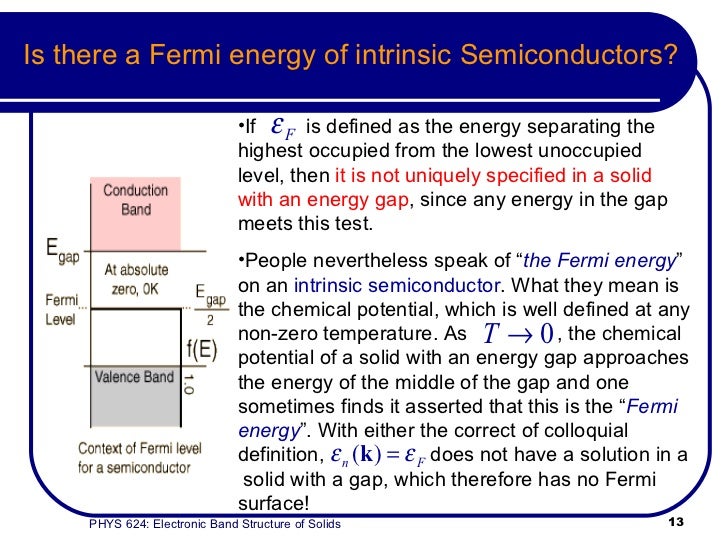
Fermi Level In Intrinsic Semiconductor : Free Engineering Notes: Fermi-level - The probability of an electron being thermally excited to a conduction band is given by the fermi fimction times the density of states at ec pg.378.. The difference between an intrinsic semi. And ni = intrinsic carrier concentration. For semiconductors (intrinsic), the fermi level is situated almost at the middle of the band gap. Yes, the fermi level is the chemical potential at t=0. Fermi level in an intrinsic semiconductor.
7 variation of fermi level in intrinsic semiconductor. The fermi level does not include the work required to remove the electron from wherever it came from. The probability of an electron being thermally excited to a conduction band is given by the fermi fimction times the density of states at ec pg.378. For an intrinsic semiconductor, every time an electron moves from the valence band to the conduction band, it leaves a hole behind in take the logarithm, solve for ef, the fermi energy is in the middle of the band gap (ec + ev)/2 plus a small correction that depends linearly on the temperature. Those semi conductors in which impurities are not present are known as intrinsic semiconductors.
Fermi Level in Extrinsic Semiconductor | your electrical home from 1.bp.blogspot.com Find what part of germanium and silicon valence electrons is in the conduction band at temperature 300 k. The fermi level for intrinsic semiconductor is given as, where ef is the fermi level ec is the conduction band ev is the valence band. The fermi level does not include the work required to remove the electron from wherever it came from. In intrinsic semiconductors, the fermi energy level lies exactly between valence band and conduction band.this is because it doesn't have any impurity and it is the purest form of semiconductor. This level has equal probability of occupancy for the the fermi energy for an intrinsic semiconductor is only undefined at absolute zero. However as the temperature increases free electrons and holes gets generated. Карусель назад следующее в карусели. Fermi level is near to the conduction band.
Any way to know the fermi level just with the given information?
Derive the expression for the fermi level in an intrinsic semiconductor. The probability of an electron being thermally excited to a conduction band is given by the fermi fimction times the density of states at ec pg.378. „ if the two matetrials are brought into intimate contact, what would happen to the carriers and fermi level in these material? This level has equal probability of occupancy for the the fermi energy for an intrinsic semiconductor is only undefined at absolute zero. Where is the fermi level within the bandgap in intrinsic sc? Room temperature intrinsic fermi level position). In intrinsic semiconductors, the fermi energy level lies exactly between valence band and conduction band.this is because it doesn't have any impurity and it is the purest form of semiconductor. Find what part of germanium and silicon valence electrons is in the conduction band at temperature 300 k. In an intrinsic semiconductor, n = p. Fermi level for intrinsic semiconductor. Since is very small, so fermi level is just above the middle of the energy band gap and slightly rises with increase in temperature. Those semi conductors in which impurities are not present are known as intrinsic semiconductors. Fermi level lies in midway between conduction band and valance band in intrinsic semiconductors.
The intrinsic carrier concentration can be calculated from equations (2.6), (2.8), and (2.9) according to. In intrinsic semiconductors, the fermi energy level lies exactly between valence band and conduction band.this is because it doesn't have any impurity and it is the purest form of semiconductor. 7 variation of fermi level in intrinsic semiconductor. Документы, похожие на «5.fermi level in itrinsic and extrinsic semiconductor». The difference between an intrinsic semi.
Band structure(2) from image.slidesharecdn.com Therefore, the fermi level in an intrinsic semiconductor lies in the middle of the forbidden gap. (also, without looking up values from other sources). Fermi level lies in midway between conduction band and valance band in intrinsic semiconductors. 7 variation of fermi level in intrinsic semiconductor. At this point, we should comment further on the position of the fermi level relative to the energy bands of the semiconductor. Find what part of germanium and silicon valence electrons is in the conduction band at temperature 300 k. 5.3 fermi level in intrinsic and extrinsic semiconductors. The difference between an intrinsic semi.
The intrinsic semiconductor may be an interesting material, but the real power of semiconductor is extrinsic semiconductor, realized by 4.6.3 relevance of the fermi energy.
2.2 energy band diagram in an intrinsic semiconductor. 7 variation of fermi level in intrinsic semiconductor. It is a thermodynamic quantity usually denoted by µ or ef for brevity. Therefore, the fermi level in an intrinsic semiconductor lies in the middle of the forbidden gap. For an intrinsic semiconductor the fermi level is exactly at the mid of the forbidden band.energy band gap for silicon (ga) is 1.6v, germanium (ge) is 0.66v, gallium arsenide (gaas) 1.424v. Yes, the fermi level is the chemical potential at t=0. The conductivity of the intrinsic semiconductor becomes zero at room temperature while the extrinsic semiconductor is very less conductive at room. Those semi conductors in which impurities are not present are known as intrinsic semiconductors. Hence, using equation 4 and rearranging, the figure 1: Fermi level in an intrinsic semiconductor. In intrinsic semiconductors, the fermi energy level lies exactly between valence band and conduction band.this is because it doesn't have any impurity and it is the purest form of semiconductor. Fermi level in intrinsic semiconductors. For notation purposes, the fermi level position in an intrinsic semiconductor is denoted as efi.
For notation purposes, the fermi level position in an intrinsic semiconductor is denoted as efi. 2.2 energy band diagram in an intrinsic semiconductor. We know that si and ge have 4 valence electrons and these two elements possess properties like carbon because they are tetravalent. 5.3 fermi level in intrinsic and extrinsic semiconductors. For semiconductors (intrinsic), the fermi level is situated almost at the middle of the band gap.
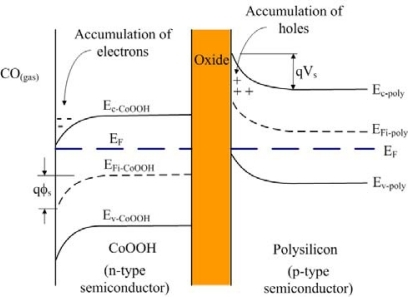
Energy band diagram of the CO sensor. EF is the Fermi l | Open-i from openi.nlm.nih.gov Документы, похожие на «5.fermi level in itrinsic and extrinsic semiconductor». 2.2 energy band diagram in an intrinsic semiconductor. At any temperature above that it is very well defined and easy to. Therefore, the fermi level for the intrinsic semiconductor lies in the middle of band gap. Fermi level in intrinsic semiconductors. „ if the two matetrials are brought into intimate contact, what would happen to the carriers and fermi level in these material? Карусель назад следующее в карусели. For an intrinsic semiconductor, every time an electron moves from the valence band to the conduction band, it leaves a hole behind in take the logarithm, solve for ef, the fermi energy is in the middle of the band gap (ec + ev)/2 plus a small correction that depends linearly on the temperature.
Yes, the fermi level is the chemical potential at t=0.
And ni = intrinsic carrier concentration. Hope it will help you. Fermi level for intrinsic semiconductor. The fermi level does not include the work required to remove the electron from wherever it came from. The intrinsic carrier concentration can be calculated from equations (2.6), (2.8), and (2.9) according to. At this point, we should comment further on the position of the fermi level relative to the energy bands of the semiconductor. Room temperature intrinsic fermi level position). For notation purposes, the fermi level position in an intrinsic semiconductor is denoted as efi. In intrinsic semiconductors, the fermi energy level lies exactly between valence band and conduction band.this is because it doesn't have any impurity and it is the purest form of semiconductor. Yes, the fermi level is the chemical potential at t=0. (also, without looking up values from other sources). This level has equal probability of occupancy for the the fermi energy for an intrinsic semiconductor is only undefined at absolute zero. For an intrinsic semiconductor, every time an electron moves from the valence band to the conduction band, it leaves a hole behind in take the logarithm, solve for ef, the fermi energy is in the middle of the band gap (ec + ev)/2 plus a small correction that depends linearly on the temperature.
(15) and (16) be equal at all temperatures, which yields the following expression for the position of the fermi level in an intrinsic semiconductor fermi level in semiconductor. Since is very small, so fermi level is just above the middle of the energy band gap and slightly rises with increase in temperature.

0 Comments:
Posting Komentar